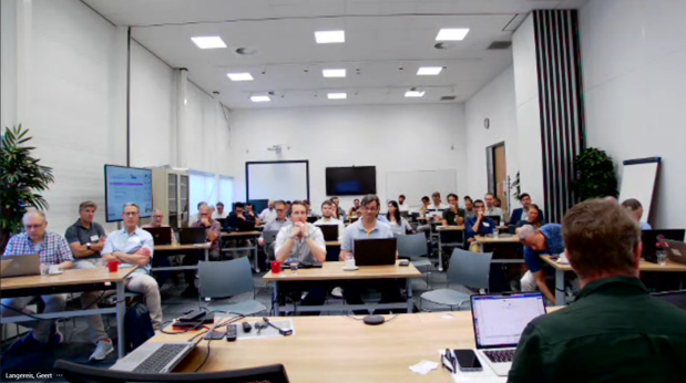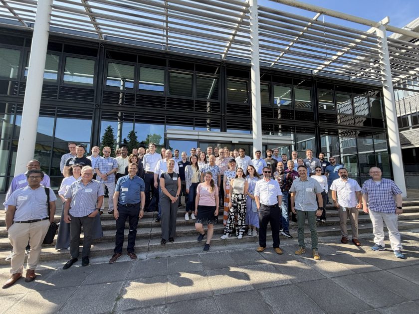
On 23 and 24 June 2026, Romans Maļiks, a researcher at the Institute of Electronics and Computer Science (EDI), took part in the kick-off meeting of the TREASURY project in Eindhoven, the Netherlands. The project aims to boost the competitiveness of integrated circuit design and manufacturing to strengthen the capacity, quality and security of European chip production. Within the project, EDI is developing a process framework for generating wafer microscopy images containing anomalies.
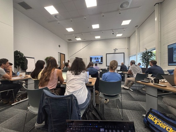
At the event, which brought together more than 40 partners from across Europe, Romans represented the institute and presented the EDI team, its members, planned contribution and areas of expertise. Following lively discussions, on the second day one of the world’s leading integrated circuit manufacturers (ams OSRAM) invited Romans to give a joint presentation, drawing attention to the fact that obtaining sensitive and confidential data (microscopy images of chips) from IC manufacturers requires particular care. Only this way can developers of AI tools (including EDI) receive and use such data for the successful delivery of the project.
The discussions addressed challenges relating to the geopolitical situation, the impact of artificial intelligence on the IC industry, and data confidentiality. As a result, contacts were established with companies widely recognised in the IC industry, such as ams OSRAM Austria, X-FAB and Silex, as well as with Simplan, Accenture, CSEM and other partners, with talks covering the project’s planned activities and latest developments.